Thin-film electronics and waterproof paper with the 2018 winner innovation
Atomic layer deposition (ALD) is one of the single most important Finnish inventions of all time. Today, ALD applications are everywhere.
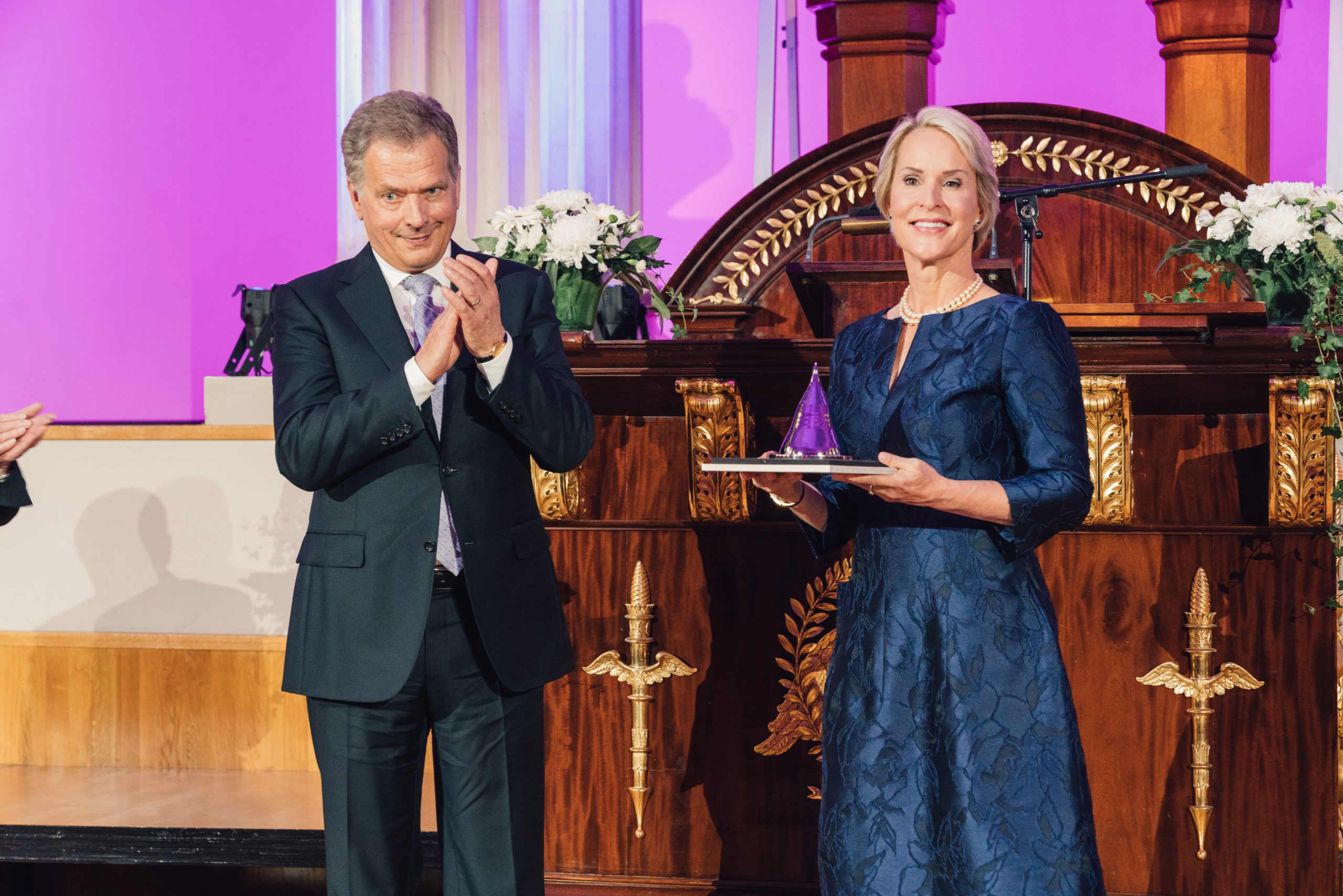
The technique involves coating structures with thin films one atomic layer at a time. In practice, the extremely thin films needed to insulate or conduct electricity in microcircuits and memory components can only be made using this technology. Tuomo Suntola received the Millennium Technology Prize for his invention in 2018.
Today, ALD applications are everywhere. Smartphones, for example, contain a huge number of electronic components featuring thin films. New applications are emerging all the time.
Advances in the measurement of film layers
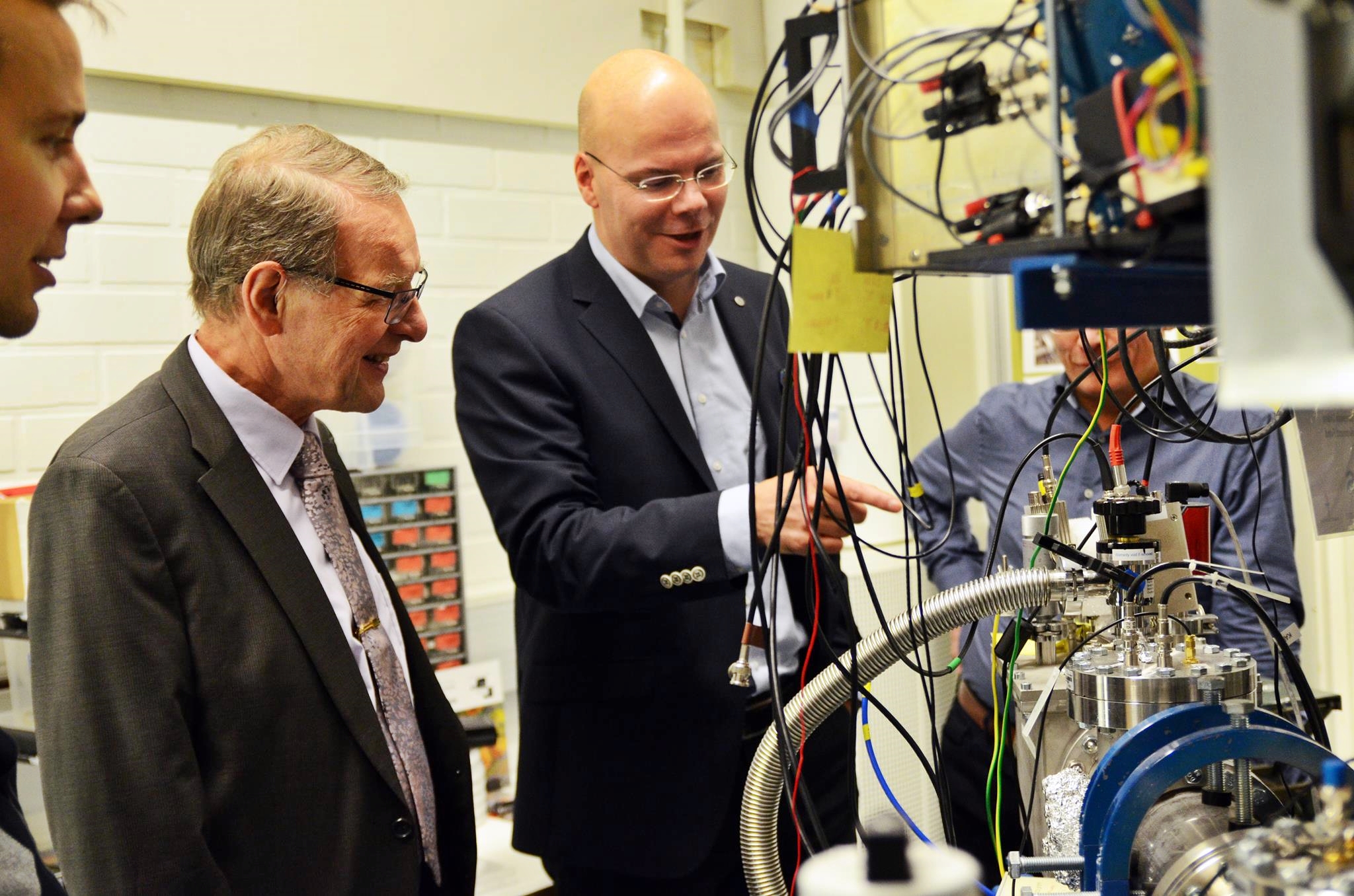
Professor Timo Sajavaara from the University of Jyväskylä (UJY) develops both new materials and material research methods.
“Our focus is on thin films grown using ALD”, Sajavaara says.
UJY specialises in measuring the exact composition of thin films. The university’s researchers regularly receive requests for assistance not just from other research institutions but also businesses.
In ALD, chemical reactants are pulsed alternatively in a reaction chamber and then chemisorb in a saturating manner on the surface of the substrate, forming a chemisorbed monolayer. The film thickness is controlled by varying the number of precursor cycles. Patterns can be created by covering parts of the substrate with a protective agent for the duration of the precursor cycle, which is rinsed off afterwards.
“The most advanced microelectronic chips manufacturing processes can involve as many as 70 different ALD steps” Sajavaara says.
Each layer must be clean and only contain the desired elements. Errors in individual layers can make the entire wafer of microchips unusable. If, for example, only some layers are meant to be conductive, the layers in between must be properly insulated.
“We are now able to measure whether each nanoscale structure only contains the elements that it is supposed to contain”, Sajavaara explains.
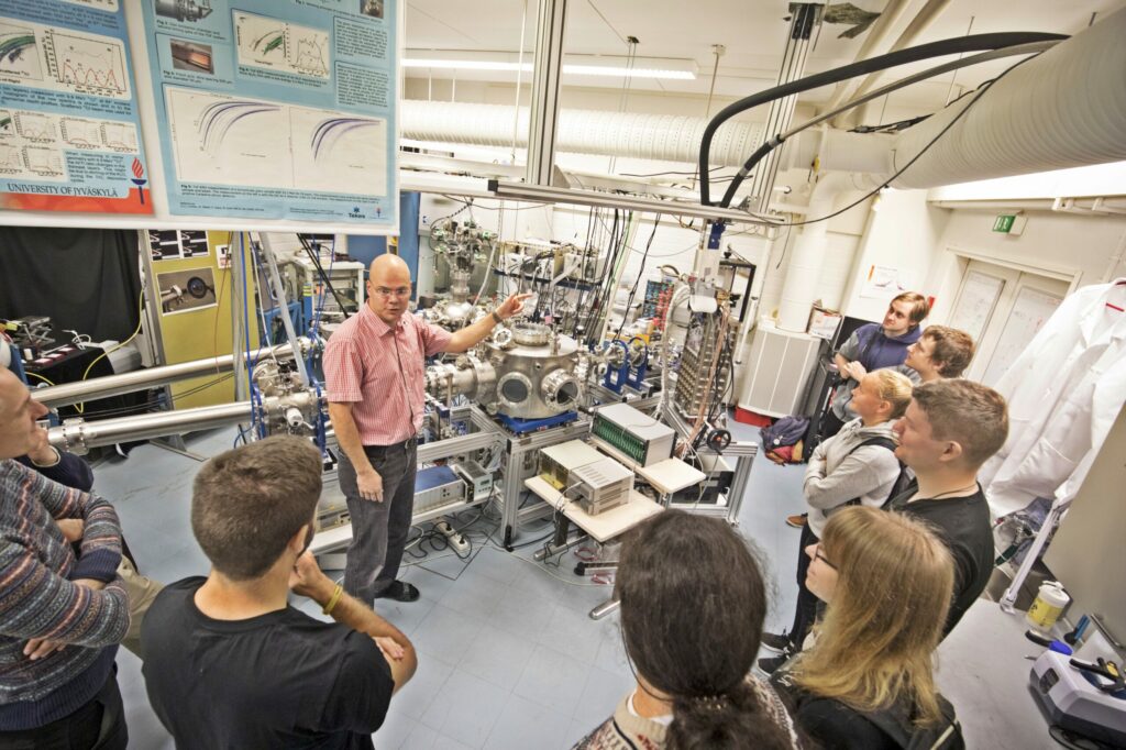
Sajavaara’s team of researchers use ion beams to study layer compositions. The technique involves shooting ions, i.e. electrically charged atoms or molecules, at the layers. The researchers then use instruments to study the directions in which the ions disperse from the substrate or whether X-rays or light are produced by ion collisions. This allows them to determine the elemental composition of the layers from hydrogen to bismuth. The analysis also shows them whether there are any defects in the crystalline layers.
Substitutes for plastic and detection of art forgeries
This millennium has turned ALD into a multifunctional technology tool without which we would not have, for example, many implantable medical devices or LED lights. UJY is also experimenting with the latest ALD applications to design a wide variety of new products with commercial partners.
The renewable energy industry relies heavily on thin-film technology.
“We have, for example, partners in the packaging industry with whom we are investigating new ways to coat paper so as to make it waterproof. This would make it possible to replace plastic containers with paper alternatives and reduce the number of plastic layers in existing paper-based products.”
One of the most important application areas of ALD is the battery industry. The need for batteries is increasing rapidly with the electrification of cars, and the excess electricity produced by wind and solar power plants needs to be stored somewhere for use on windless and dark days.
“Modern, more durable batteries are completely solid inside. ALD is a promising technique for solid-state battery fabrication”, Sajavaara says.
The renewable energy industry relies heavily on thin-film technology.
“ALD is already used in solar power plants, which are becoming increasingly common, and we have ideas on how to use ALD coatings to make wind turbine blades dirt-repellent and icephobic”, Sajavaara explains.
Ion beams are also being used to analyse substrate composition in the most diverse contexts. UJY has used ion beam technology to study everything from the composition of meteorites to the materials used in paintings to detect forgeries. UJY’s researchers have also received funding from the Academy of Finland to investigate changes in nanostructures embedded in an ALD film using ion beam bombardment.
Funding from the Academy of Finland
Sajavaara’s team of ALD researchers have also received funding from the Academy of Finland.
“The Academy is our most notable external source of funding”, Sajavaara says.
Sajavaara is especially pleased with how transparently the Academy distributes its research grants.
“The Academy listens to the applicants. If the research community finds a procedure cumbersome, the Academy is happy to revise it.”
Text: Visa Noronen
Pictures: Inka Pasanen, Petteri Kivimäki, University of Jyväskylä (UJY)